Hardware
Motivation
The Protos Simulator is intended to provide a HW platform for testing embedded software. It can help stimulating and measuring all kinds of signals which are typically generated or measured from embedded targets.
The Protos Simulator can be used from the very beginning of an embedded software project by providing simple analog or digital signals or measuring those such signals. The basic idea is to run the target software on the Evaluation kit of your choice. The Simulator is prepared to take STM32 Nucleo boards or some Discovery boards directly. If you use other controllers an adaptor may necessary.
This document describes the Protos Simulator HW and all the features.
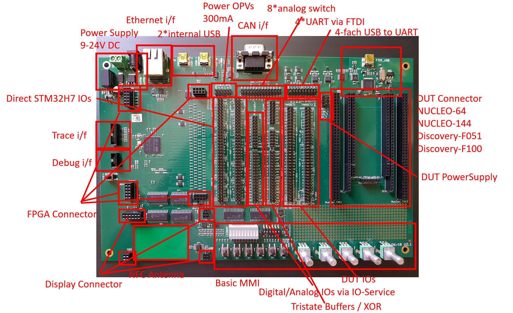
Power Supply
The board requires a DC-Voltage from 9V to 24V. The input voltage can be delivered via screw terminals or round plug. The connectors are simply switched in parallel, do not use both at the same time.
The power supply delivers:
-
5V output max 2A
-
3,3V output max 1A
-
3,3V analog output 150mA
The 3,3V LDOs are driven from the 5V DC/DC converter. So the 2A is the maximum total current that can be provided.
Simulation Controller
The simulation controller is a STM32H743 microcontroller from ST-Microelectronics running at 400Mhz. The base of all the measurement and stimulation capabilities are based on the peripherals of this microcontroller. However some of the peripherals are used for internal purposes to extend the capability of the board.
A full description of the microcontroller can be found at the ST homepage. All datasheets can be downloaded there.
The following interfaces are used internally:
-
SPI1 ⇒ analog outputs
-
SPI3 ⇒ digital IOs
-
SPI4 ⇒ MMI extension slot
-
SPI5 ⇒ SPI flash or user switchable via SW
-
SPI6 ⇒ FPGA slot or user switchable via SW
-
I2C1 ⇒ MMI interface
-
ADC1 ⇒ Potentiometer inputs
-
QSPI dual bank ⇒ FPGA slot
-
LPTIM1 ⇒ MMI extension slot
For debugging the standard Cortex-M debug connector is provided (10-polig). Additionally the standard Cortex-M trace connector is provided (20-polig).
For further information please refer to the Cube project of the Template project.
Digital IOs
To extend the amount of simple digital IOs available, two port extender chips MCP23S17 have been used. The chips are configured to provide 16 inputs and 16 outputs. SPI3 drives the port extenders. The SPI interface is configured to send and receive every 12us all IOs to the H7 micro via DMA. So setting an output is just a memory access. The physical output will be set max 12us later.
The inputs will be updated in the same timeframe. However the memory represantation of this inputs will be polled every ms (max 100us).
Analog outputs
Two DAC128S085 chips from TI are used to provide 16 analog outputs. The DACs are driven from SPI1. The outputs are updated every 12us via DMA. So setting an analog output is just a memory write.
The H7 also provides two analog outputs. These outputs are also connected to the analog output connector.
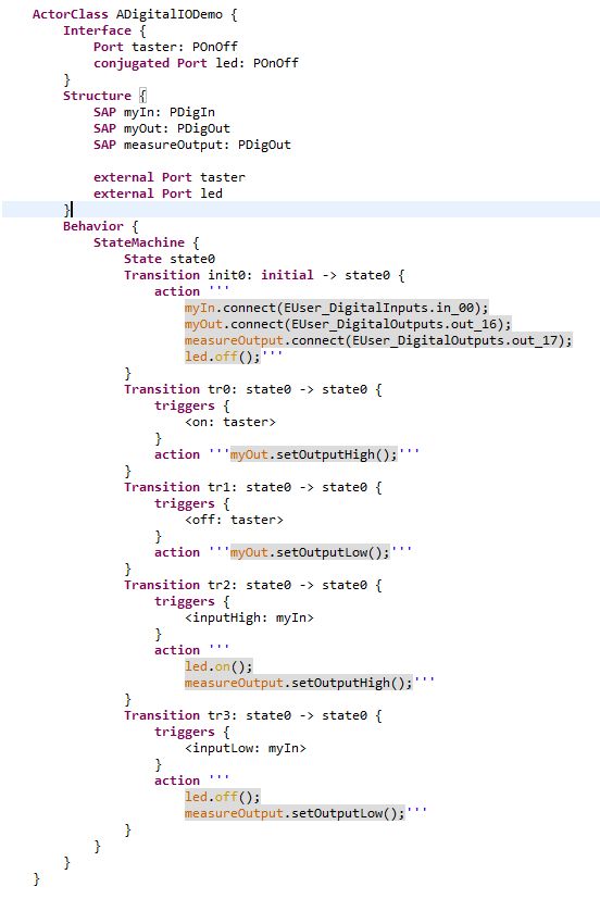
Controlling digital and analog IOs from software
As with every other signal, the digital and analog IOs are encapsulated within a HW-related actor. To avoid too many ports at the HW-Abstraction actor, the general purpose digital IOs and analog outputs are encapsulated as special actors named services.
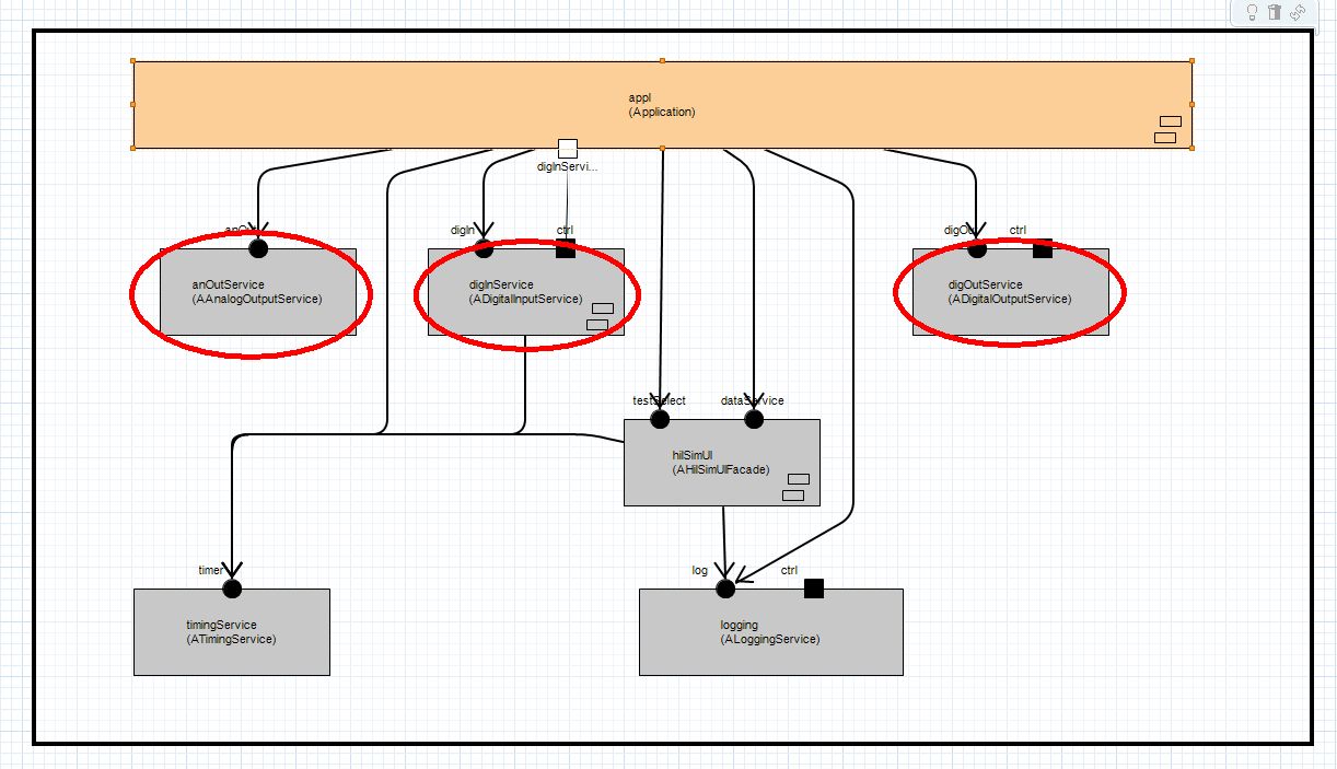
The difference between services and normal actors is that any actor within the application is allowed to use service IOs without connecting to a dedicated port. This makes its usage more flexible without the need of dedicated connections and cluttering the HW-Abstractation layer. It is best used for elements which are widely used within the application such as a clock timer, logging or large amounts of IO channels.
The language ROOM provides Service Access Points (SAP) and Service Provision Points (SPP) for the information of services.
To use an IO you should do the following steps:
-
Create an SAP. The name should represent the functionality within your model.
-
Connect to the pin. With the "connect" message you can connect a pin to your SAP. This is done via IDs which are provided via enums (in_00 ⇒ in_15; out_16 ⇒ out_32 for digital IOs, out_00 ⇒ 15 for analog outputs).
Behaviour of the IOs:
Outputs:
One SAP can be connected to one pin. If a pin is already connected and any other actor tries to connect to the same pin, the last connection get the highest priority. The SAPs that are already connected will be disconnected and they will be informed about the disconnection with the "disconnect" message. This behaviour is the same for analog and digital outputs.
Inputs:
Multiple SAPs can be connected to the same input pin. Each connected SAP will be informed whenever an input changes.
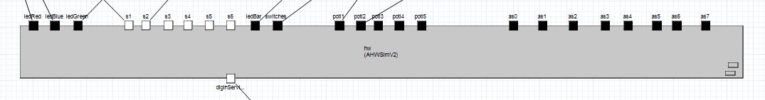
MMI
The MMI consists of:
-
3 LEDs (read, blue, green)
-
LED bar (10 red LEDs)
-
Dipswitch bar (6 switches)
-
6 single buttons
-
5 potentiometers
The LEDs, switches and buttons are connected via 4 MCP2317 chips (I2C1). This interface runs at 400khz. Everything is updated within 1ms.
The MMI can be used to control the tests and stimuli and to show states of the target SW or the simulator itself.
Analog switches
The board provides 8 analog changeover switches (TS5A23159). The switches are controlled by software. They can be used to multiplex signals between DUT and simulator or for any other purpose. The control input of the analog switches are connected to the MCP2317 from the MMI interface. That means changing of the switches takes place with a 1ms delay.
Please note:
COMx: root
NOx:  normally opened
NCx:  normally closed
Controlling MMI and Analog switches from Software
All MMI parts are controlled via dedicated ports. In contrast to the IOServices for the general purpose IOs, you have to make a dedicated connection to dedicated elements (e.g. for controling an LED you have to connect to this port).
Also the analog switches are controlled via these dedicated ports.
Power OPVs
There are 2 TLV4112 OPVs (2 channels each). This chip can drive a max current of 300mA. These chips can be used to test brownout functionality of the target. Via solder jumper, the OPVs can be supplied with 3,3V or 5V and the gain factor can be setup via external resistors.
Tristate drivers
There are 2 AHC125 and 1 AHC126 tristate buffers mounted on the board. This can be used to provide signals that must be tristated or driven high or low. The target reset is an example of using tristate buffers
Simulated CAN interfaces
This is a special feature to simulate a UART via CAN connection. The SimCAN interfaces are basically the the same as the tristate drivers, but these drivers can be configured to behave like a CAN-driver (simply mirror the sent data back to the receiver). Configuration is done via solder bridges. Per default these drivers can be used as normal tristate buffers.
XOR Gate
For block commutated BLDC motors, the high side PWMs can be combined with a XOR to generate a one timer input signal. This is very useful to measure the overall PWM duty.
Communication interfaces
FTDI 4232
There is a FTDI4232 4 channel USB to UART chip provided. The UART outputs are accessible via jumpers and can be connected to the target or the simulator microcontroller. This interface can be used to connect the DUT (Device Under Test) to a PC to extend the testing capabilities or connect the H7 to a PC to provide a LoggingService or any other functionality. One of the UARTs (channel A) can be used to reset the simulator and bring it to boot mode. This feature can be used for remote update of the simulator SW.
CAN
The H7 CANFD interface is provided at a SUBD 9 connector. The CAN drivers are also provided so that you can connect directly a CAN interface for any purpose.
This interface is currently not supported from SW.
USB 1/2
The 2 USB interfaces are the internal USB interfaces of the H7 microcontroller. These interfaces will be used for logging and Jenkins connection.
Due to the fact that these interfaces are provided directly from the H7, they are only available as long as the simulator software is running.
Ethernet
There is also an ethernet interface provided. The H7 runs the LwIP-Stack on top of the FreeRTOS OS. Currently just ICMP is implemented.
NFC interface
There is an NFC-Tag ST25DV64K mounted. The chip can be accessed from the H7 micro via I2C1. It can be used to provide board individual configurations like a MAC address or some other HW changes that are necessary for this particular tests.
The configurations are stored in the normal NDEF format. If you run the software a virgin NFC-chip will be detected and an example NDEF record will be programmed. You can read it out via your Android mobile phone (if it provides NFC), change it and write it back. If you use the provided NDEF format, you can use a small parser to get the stored values from the NFC chip.
Yo should use the "ST25" NFC App. It is available here from the Google Play store.
8MB SPI Flash
There is an additional 8MB flash mounted. This can be used to store FPGA loads or some other test specific data (e.g. waveforms for analog signals)
Currently there is no software support available.
DUT Interface
The DUT interface basically consists of a NUCLEO-144 slot. The slot is compatible with NUCLEO-64. The NUCLEO boards are available for many STM32 microcontrollers.
For special purposes the MB913C and MB1034B boards (STM32 Discovery for F103 and F051) can be plugged as well.
All other boards must be connected via an adapter.
For further information refer to the ST homepage.
Board Configurations
Poti (Potentiometer) Configuration
Poti 2-5 are optional. It is possible to disconnect the poti from the analog input of the micro. In this case you can use the input for something else.
Closed ⇒ poti connected
| SB | GPIO | description | default |
|---|---|---|---|
SB 27 |
PC3C |
Poti 2 |
closed |
SB 28 |
PF5 |
Poti 3 |
closed |
SB 29 |
PF3 |
Poti 4 |
closed |
SB 30 |
PC0 |
Poti 5 |
closed |
I2C3
I2C3 can be connected to the FPGA slot or to the pin stripe.
| SB | GPIO | description | default |
|---|---|---|---|
SB 34 |
PH8 |
SDA connected to PH8 |
closed |
SB 35 |
PH8 |
SDA connected to FPGA |
closed |
SB 36 |
PH7 |
SCL connected to PH7 |
closed |
SB 37 |
PH7 |
SCL connected to FPGA |
closed |